Meeting Annex 1 Compliance: Overcoming Disinfectant Residue Challenges with Foamtec’s Sahara+ Wiping System

Pharmaceutical facilities face increasing pressure to meet the rigorous cleaning and contamination control requirements outlined in the revised EU GMP Annex 1. A key challenge these facilities encounter is effectively removing disinfectant residues from stainless steel and glass surfaces. Residues left behind by commonly used disinfectants can compromise product quality, pose contamination risks, and contribute to long-term degradation of critical cleanroom surfaces.
Many pharmaceutical manufacturers find themselves in a difficult position. On the one hand, they recognize the need for thorough residue removal to comply with Annex 1 requirements and ensure patient safety. On the other, validating new detergents that could aid in residue removal presents significant obstacles, including the costs and time associated with revalidation. Consequently, the industry is in search of a reliable and efficient cleaning method that ensures compliance without introducing additional complexities.
Foamtec’s Sahara+ Cleaning System offers an innovative solution that allows pharmaceutical facilities to meet Annex 1 compliance without needing new detergent validations. This two-step wiping system effectively removes even heavily stained stainless steel and glass surfaces using only deionized (DI) or water for injection (WFI) and 70% isopropyl alcohol (IPA).

The Sahara+ Two-Step Wiping System
The Sahara+ system is designed to optimize contamination control by utilizing a structured two-step approach:
Step 1: Initial Removal with Sahara Sponge Wipers
- Sahara Sponge Wipers effectively lift and absorb disinfectant residues, biofilms, and particulates from surfaces without harsh detergents. The sponge’s unique polyurethane foam composition ensures thorough removal without leaving fibers or lint behind, making it ideal for GMP cleanroom environments.
Step 2: Thorough Residue Removal with MiraWIPE or CoverMAX
- Following the initial scrubbing, the surface is wiped with MiraWIPE wipers, which provide a final polish using 70% IPA or WFI/DI water. This critical step ensures that all residues loosened by the Sahara Sponge Wipers are effectively and completely removed, leaving surfaces pristine and compliant with Annex 1 standards. The high absorbency and cleanliness of MiraWIPE prevent residue redeposition, ensuring optimal surface integrity.

Compliance with Annex 1 and Preventing Surface Degradation
The Sahara+ system aligns perfectly with the stringent cleanliness and contamination control expectations of Annex 1:
- Ensuring Effective Residue Removal: The two-step process eliminates disinfectant residues that can otherwise accumulate and compromise cleanliness.
- Reducing Cross-Contamination Risks: Using Sahara+ allows facilities to maintain validated cleaning processes without introducing new chemicals that could require extensive validation.
- Preventing Surface Degradation: Over time, residual disinfectants can contribute to surface roughness and rust formation, particularly on stainless steel. Sahara+ helps prevent these issues by thoroughly removing residues with a gentle yet effective cleaning action, preserving surface integrity in GMP cleanrooms.


A Practical and Cost-Effective Solution
By implementing the Sahara+ wiping system, pharmaceutical manufacturers can achieve compliance with Annex 1 without the burden of validating new detergents. This solution provides an efficient and cost-effective way to maintain the highest standards of cleanliness while protecting critical equipment and infrastructure from premature wear and contamination-related failures.
In an era of increasing regulatory scrutiny, Sahara+ offers a proactive approach to cleanroom maintenance, allowing facilities to stay ahead of compliance challenges and focus on producing safe, high-quality pharmaceutical products.
Conclusion
Meeting Annex 1 requirements for cleaning disinfectant residues no longer needs to be a challenge fraught with complexities. Foamtec’s Sahara+ Cleaning System provides a validated, detergent-free solution that removes stubborn residues, ensures regulatory compliance, and safeguards cleanroom surfaces against degradation. This innovative approach allows pharmaceutical manufacturers to streamline their cleaning processes and enhance overall operational efficiency in GMP cleanrooms.
 The
The 
 industry. Thus, stable and highly accurate flow measurement is essential for many semiconductor manufacturing steps. Non-contact clamp-on flow meters such as SEMIFLOW CO.65 have proven to fulfill this demanding task reliably.
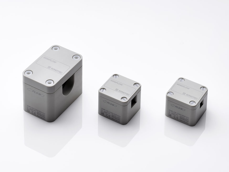 The ultrasonic sensors measure through the wall of the tube or pipe and substantially reduce the risk of contamination or leakage of hazardous fluids. With the