


Product Type: Metrology & Handling
Application: Scanning Electron Microscopy
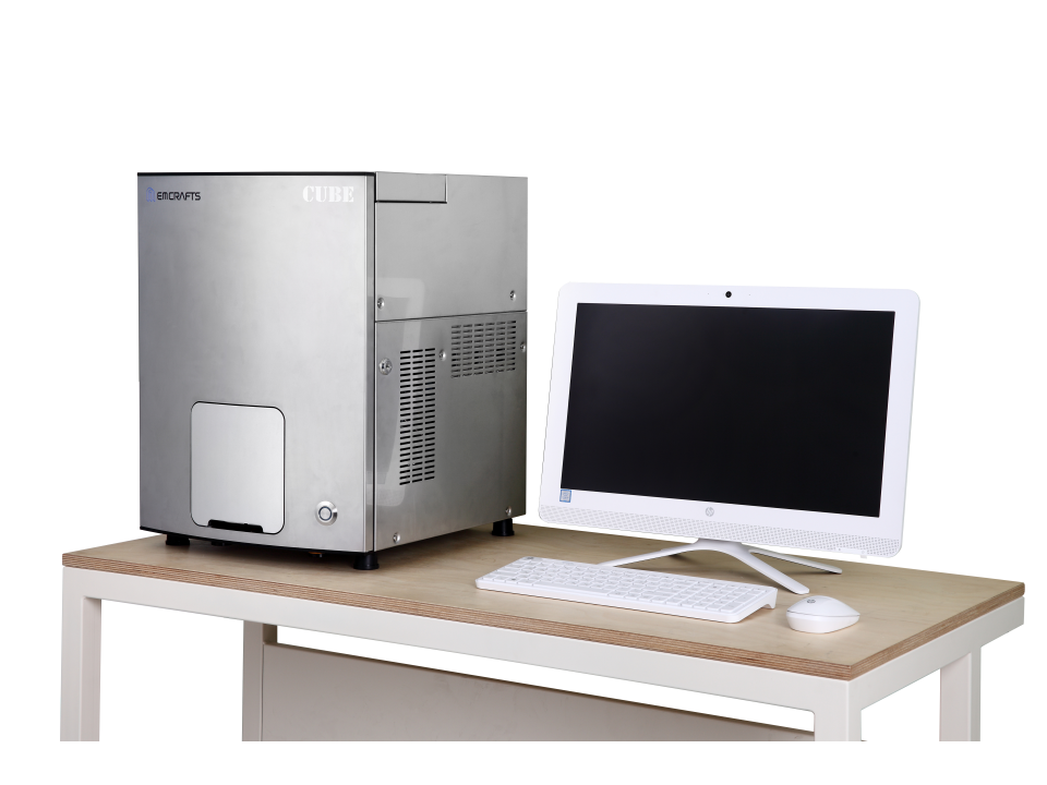
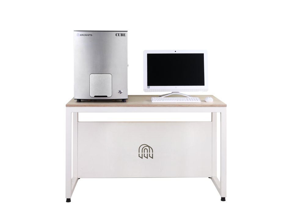
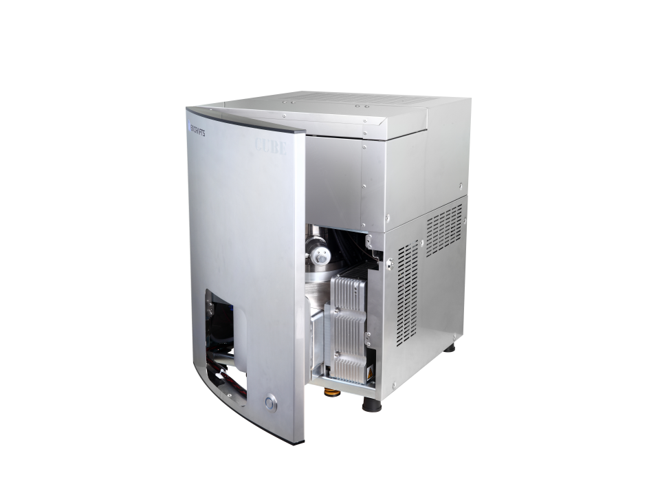
EMCrafts CUBE II Series:
Scanning Electron Microscope (SEM) with World-Class Performance
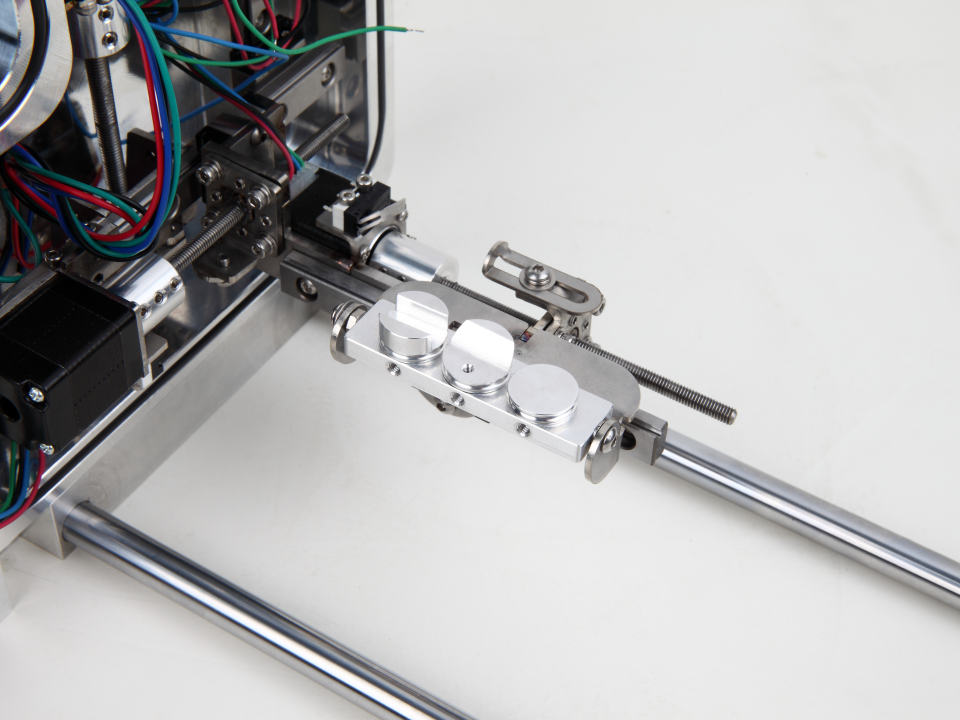
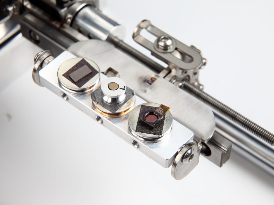
- Automatic stage & 4CH BSE as a basic option
- Lightweight & High productivity
- Integrated EDS System (Option)
- DIY installation
Advantages
- Simple and Intuitive User Interface for Everyone
- 65 kg portable Tabletop SEM
- 5-Axis Stage System
- Maximum Sample Size: Horizontal: 140 mm, Vertical: 80 mm
- Magnification: 10–200,000x
- Automatic Functions To Minimize Repetitive Tasks – Auto Focus, Auto Brightness & Contrast, Auto Gun Alignment, Auto Saturation
- High Resolution Imaging – 5.0 nm (SE Image) / 6.0 nm (BSE Image)
- Rapid analysis by exchanging specimen within 90 sec – Vacuum ready within 90 sec – Ventilation ready within 10 sec
- 4CH BSED as a basic option(Combo, Topo)
- Various kinds of specimens can be analyzable with optional detectors – EDS (All-in-one Model of SEM-EDS) *Oxford, Bruker, EDAX, Thermo compatible, Auto Rotation, Auto Tilt, Chamber Camera, Navigation
| Stage | 5-axis Stage -X: 42 mm (Motorized) -Y: 42 mm (Motorized) -Z: 5 ~ 53 mm (Motorized) -T: -90° ~ 90° (Manual) -R: 360° (Beam Rotation) |
||
| Vacuum Mode | High Vacuum Mode (<9×10⁻³ Pa) Charge Reduction Mode |
||
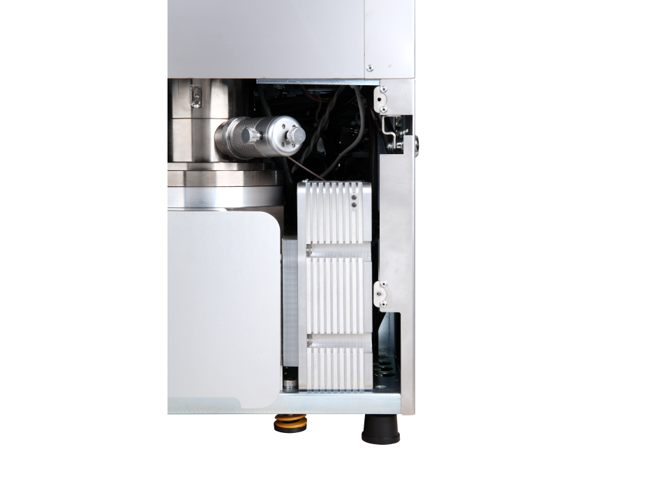
| Vacuum System | -Fully Automated Evacuation System -Turbo molecular pump (Vacuum ready within 90 sec) -Rotary vane pump -Electrical valve system |
||
| Electron Gun | Pre-centered Tungsten Filament | ||
| Detector | SE Detector 4CH BSE Detector | ||
| Resolution | 5.0 nm (SE Image at 30 kV) | ||
| Magnification | 10–200,000x | ||
| Acceleration Voltage | 1 kV ~ 30 kV | ||
| Image Shift | 100 μm | ||
| Maximum Sample Size | Horizontal: 140 mm; Vertical: 80 mm | ||
| Working Distance | 5 ~ 53 mm | ||
| Sample loading Time | 90 sec (Vacuum) 10 sec (Vent) | ||
| Automatic Function | Auto Brightness & Contrast, Auto Focus, Auto Gun Alignment, Auto Saturation, Auto Filament, Bias | ||
| Image Format | JPG, TIFF, BMP, PNG | ||
| Display Mode | Focus Mode : 320 x 240 pixel, Resizable Preview Mode: 800 x 600 Slow Mode: Applicable to both preview and focus mode Photo Mode: Up to 3200 x 2400 |
||
| Dimension(mm) | W x D x H = 410 mm x 440 mm x 520 mm, 65 kg | ||
| Operation Device(PC) | Windows 10-based All-in-One 21.5” Workstation, 100% controlled by keyboard and mouse | ||
| Optional Devices | EDS (All-in-one Model of SEM-EDS), Auto Rotation, Auto Tilt, Chamber Camera, Navigation *Oxford, Bruker, EDAX, Thermo compatible |
||
| Power Supply | Single Phase: 100–240 VAC, 50 / 60 Hz, 1 kVA | ||
file_downloadcube-ii-table-sem-for-web.pdf
There are currently no videos available.
SEM is widely used across various fields to produce unprecedented images of the microscopic and nanometric world.
Our family of SEM models is widely used in research fields and industry applications such as semiconductors,
flat-panel display, and nanotechnology labs.
- Quality control of electronic circuits and semiconductor parts
- Observation of microstructure of Secondary cell, CNT (Carbon Nano Tube), Solar Cell, Wafer, Bonding Wire, LED,
Nanotech