


Product Type:
Equipment
Application:
Dry Processing & UHP
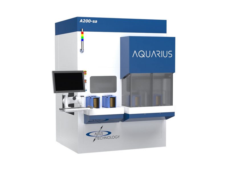
Product Description:
The C3100 Automatic CO2 Filmframe Wafer Cleaning System from IMT is designed to deliver precise and efficient cleaning for filmframe wafers, ensuring optimal performance in semiconductor manufacturing. With two cleaning chambers, the system enhances throughput and efficiency, allowing for continuous operation. By utilizing advanced CO2 cleaning technology, it effectively removes a wide range of contaminants from wafer surfaces without causing any damage.
Key Features:
- Precision Cleaning: The C3100 targets and removes particles, and residues from delicate filmframe wafers, preserving surface integrity and improving wafer quality.
- Automated Process: Featuring an automated loading and unloading system, the C3100 enhances productivity while minimizing manual intervention and reducing operational costs.
- High Efficiency: The system offers a fast, thorough cleaning process with two cleaning chambers, ensuring high throughput and making it ideal for semiconductor production environments.
- User-Friendly Interface: With an intuitive control system, the C3100 is easy to operate, allowing for efficient integration into existing workflows with minimal training.
The C3100 Automatic CO2 Filmframe Wafer Cleaning System is the perfect choice for manufacturers aiming to improve cleaning precision and efficiency in their semiconductor processes.
CO₂ Cleaning Technology
CO₂ Cleaning Mechanism
- Physical Blasting
Dry ice particles are accelerated by compressed air and collide to the surface - Thermal shock
Sublimation heat of -78.5℃ shrinks foreign matters and causes cracks - Sublimation expansion
Expands volume to 800 times and breaks the boundary - Ablation
Uses the air pressure of the high-speed compressed air to remove
Dry-ice (Size: variable) + CDA (Clean Dry Air)

Advantages of the CO2 Cleaning
- Free from chemicals/water
- No need for an additional drying process
- Minimum secondary waste after cleaning
- Free from surface damages
- Easy automation
There are currently no downloads available.
Applications in Semiconductor/MEMS:
- TSV
- MEMS Wafer Particle Removal
- Bare Wafer Epoxy
- PR residues Cleaning or Organics Contaminations and residues Cleaning
- Bump Wafers and Removal of Bond Residues
- Glass Carrier Cleaning
- Wafer Backside Cleaning
- EdgeContaminations Cleaning
- Framed Wafers Cleaning after Dicing