


By KOVIS Technology
Supplier Info
Produkttyp:
Metrology & Handling
Anwendung:
Dimensionelle Wafer-Messtechnik
Produktbeschreibung:
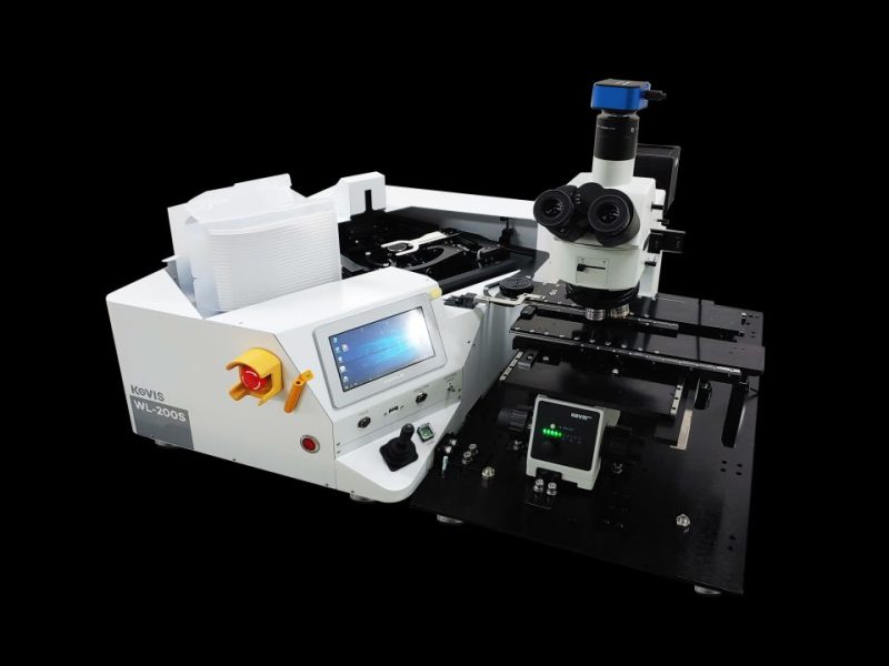
Der NANOMEZ® RT-3500 ist ein speziell entwickeltes Hybrid-Messtechniksystem, das die automatische Messung der Wafer-Form, submikroskopischer 3D-Strukturen und Rauheit in einem einzigen System ermöglicht.
Insbesondere nutzt es eine Multi-Sensor-Technologie, bestehend aus konfokalen Sensoren, Kapazitätssonden und IR-Transmissionssensoren zur Messung von Wafer-Dicke, Verzug und Biegung. Zusätzlich kommt ein WLI (Interferometer) FOV-Sensor zur Messung der nanoskaligen Oberflächenrauheit und zur 3D-tomografischen Analyse zum Einsatz. Dank dieser leistungsstarken, kombinierten Multi-Sensor-Technologie können Nutzer eine umfassende One-Stop-Messung für Wafer im Front-End der Wafer-Packaging-Prozesse durchführen.
Die Kombination aus verschiedenen kontakt- und berührungslosen Messtechniken ermöglicht Ingenieuren, Mikro- und Nano-Oberflächenanalysen und Messungen präzise und effizient durchzuführen.
- Automatische Wafer-Dickenmessung & Optischer 3D-Profiler
- WLI (Interferometer) und berührungslose Dickenmessung
RT3500 Systemspezifikation
Main Operation Program Function:
- Program one-click auto start / Button box (option)
- Recipe programming, infinite recipe creation
- Measuring points set-up on wafer Image
- Automatic measurement with pre-programmed recipe
- Wafer ID, Lot#, User name and other category DB
- Measured data Display, Saved & Export in CSV
- Capable to call saved data in specified folder (File name of LOT NO.)
Wafer Size: Small piece, 4″, 6″, 8″, 12″ wafer (custom design available)
Wafer Chuck: Steel Vacuum chuck with sensor holes & ESD coating
Wafer Handling: Manual loading on motorized XY stage
XYZ Stage & work table: 350 x 350 mm Servo linear XY stage / 65 mm Z-axis/ Multi-point sensor hole work table
Stage Accuracy: ± 10 ㎛ / 5 ㎛ / 1 ㎛ / 0.1 ㎛
Anti Vibration Support: Passive anti-vibration table (Active option)
HW System Frame: Steel & Granite frame
Operation Program: Windows 7-based KOVIS metrology studio, Nanomez V.3.5
PC: Industrial PC, minimum 2.2 GHz Intel i7, 32 GB Memory, 256 GB SSD
Accessories: 21″ single monitor, keyboard, mouse and holder arm
System Size: 860W x 1230D x 1350H mm (System size changeable)
Weight: 350 kg or more
Electrical: 220 volts single phase at 4.9 KVA (peak), 50/60 Hz
Vacuum: 0.5 Mpa
Exhaust: One 10.16 cm (4″) diameter port on the floor adjacent to the instrument
Environmental: Operating Temp : +18 to +24°C
Metrology: Wafer Thickness & Warpage Measurement Module (WT3500)
Capability of WT3500: Automatic Wafer Thickness (TTV) measurement
Optional Function: Warpage/ Bow measurement /Bump Height I Strip Thickness I Die Height ( Manual / Auto )
Edge Chip and Crack
Measurable Materials:
• Bare wafer (Pattern, Si, Ge, GaAs, InP, Sapphire), Glass, Solar cell, FPD □
• Wafer on tape(ring framed) / Bump wafers / Strip, PCB /
Metrology Sensors (option):
CCP Capacitance sensor
CLS Confocal sensor
Vision A/F height measurement
CIR Transmittance sensor
CAS High precision micro air touch sensor
Measuring Range: 10 ㎛ ~ 790 ㎛ thickness (Max. 1,500 ㎛ including tape thickness)
Measurement Resolution: 0.01 ㎛
Measurement Accuracy: ± 0.5 ㎛
Repeatability: ± 0.25 ㎛
TTV (Total Thickness Variation): TTV (Total Thickness Variation)
Optional (Bump Height): Bump sizes : 50~500 ㎛
Measurement method : Manual by vision auto-focus
Calibration Method(Baseline): Silicon master piece, Si Certification from authorities
Auto-map Point (Thickness): 89 points for 12” and 37 points for 8” wafers
Software: RT-3500 main program
Metrology: 3D Profilometry Module (WL3500)
Capability of WL3500: Nano~Micro 3D profilometry
Vertical Resolution: VSI, VEI < 0.5 nm, VPI < 0.1 nm 3D profiler module
Lateral Resolution: 0.05~7.2 µm (Depends on magnification)
Height Repeatability: ≤0.1% @ 1σ (Standard Height)
Objective Lens: 5 Seletable (Automatic)
Zoom Lens: 2 Selectable (Automatic)
Camera Format: 1/2″ Mono CCD (option: 1/3″ or 2/3″)
Scan Method: Piezo @ Capacitive Sensor Closed loop (Linearity error ≤ 0.05%)
Scan Range: ≤150 µm (option ≤300 µm@Piezo or 10 mm@Motor)
Scan Speed: 7.5 µm/sec(1x) / 22.5 µm/sec(3x)
Illumination: White LED
Filter: 2 or 3 Filter (Automatic)
Z Axis Stroke: 50/ 100 mm (Automatic)
Tilt Aixs Stroke: ±2°/ 3°/ 6°(Manual)
Max Workpiece Load: ≤ 10 kg
Auto Focus: Optional
Stitching: Yes
Software: Surface View / Surface Map @ Windows 10 64-bit.
There are currently no videos available.
Thickness & Warpage
• Thickness, TTV
• Bow & Warpage
• Bare Si, Patterned, Framed, and Bump wafers
and Bump wafers on tapes
• Edge chip and edge crack (Optional)
• Si, Ge, GaAs, InP, Glass, Solar cell, FPD
• Capable to measure wafer thickness with the
tapes (clear, opaque, milky)
• Ultra Thin Wafer Measurement ability up to 20 ㎛ wafer or thicker
• Thin film thickness option
Roughness & 3D Topography
• Roughness Measurement by FOV Sensor
• Surface 3D profilometer
• Height Resolution, 0.1nm Max
• The same resolution for different object lenses
• High speed, High accuracy, High-resolution surface 3D topography measurement
• Excellent measurement performance for the transparent/ semi-transparent/milky-colored samples
• High accuracy of repeatability, accuracy, and reproductivity
• Height, Step height, Depth, Line, Circle, Round, Angle, Width, Distance Measurement
• Roughness of line, FOV, measurement of waveform
• Scratch, abrasion and defects analysis
• Area, and volume measurement