


By KOVIS Technology
Supplier Info
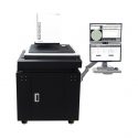
Product Type: Metrology & Handling
Application: Wafer Dimensional Metrology
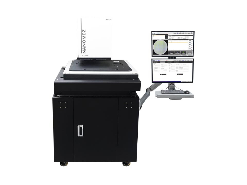
NANOMEZ® RT-3500 is a specially designed hybrid metrology system that can automatically measure wafer shape & sub-micro 3D structure and roughness in one measurement system. In particular, it uses multi-sensor technology of Confocal, Capacitance probes, and IR transmission sensors to measure wafer thickness, warpage, and bow as well as WLI (Interferometer) FOV sensor for nanoscale surface roughness measurement and 3D tomographic measurement. Its powerful combined multi-sensor technology allows users to proceed with one-stop measurement for wafers in the front-end of wafer packaging.
Combining these with various contact and non-contact metrology tools makes it easy for engineers to conduct micro- or nano-level surface analysis and measurement.
Automatic Wafer Thickness & 3D Optical Profiler
WLI (Interferometer) and Non-contact Thickness Measurement
RT3500 System Specification
Main Operation Program Function:
- Program one-click auto start / Button box (option)
- Recipe programming, infinite recipe creation
- Measuring points set-up on wafer Image
- Automatic measurement with pre-programmed recipe
- Wafer ID, Lot#, User name and other category DB
- Measured data Display, Save & Export in CSV
- Capable to call saved data in specified folder (File name of LOT NO.)
Wafer Size: Small piece, 4″, 6″, 8″, 12″ wafer (custom design available)
Wafer Chuck: Steel Vacuum chuck with sensor holes & ESD coating
Wafer Handling: Manual loading on motorized XY stage
XYZ Stage & work table: 350 x 350 mm Servo linear XY stage / 65 mm Z-axis/ Multi-point sensor hole work table
Stage Accuracy: ± 10 ㎛ / 5 ㎛ / 1 ㎛ / 0.1 ㎛
Anti-Vibration Support: Passive anti-vibration table (Active option)
HW System Frame: Steel & Granite frame
Operation Program: Windows 7-based KOVIS metrology studio, Nanomez V.3.5
PC: Industrial PC, minimum 2.2 GHz Intel i7, 32 GB Memory, 256 GB SSD
Accessories: 21″ single monitor, keyboard, mouse, and holder arm
System Size: 860(W) x 1230(D) x 1350(H) mm (System size changeable)
Weight: 350 kg or more
Electrical: 230 V single phase at 4.9 kVA (peak), 50/60 Hz
Vacuum: 0.5 Mpa
Exhaust: One 10.16 cm (4″) diameter port on the floor adjacent to the instrument
Environmental: Operating Temp: +18 to +24°C
Metrology: Wafer Thickness & Warpage Measurement Module (WT3500)
Capability of WT3500: Automatic Wafer Thickness (TTV) measurement
Optional Function: Warpage/ Bow measurement /Bump Height I Strip Thickness I Die Height ( Manual / Auto )
Edge Chip and Crack
Measurable Materials:
• Bare wafer (Pattern, Si, Ge, GaAs, InP, Sapphire), Glass, Solar cell, FPD □
• Wafer on tape(ring framed) / Bump wafers / Strip, PCB /
Metrology Sensors (option)
CCP Capacitance sensor
CLS Confocal sensor
Vision A/F height measurement
CIR Transmittance sensor
CAS high-precision micro air touch sensor
Measuring Range: 10–790 ㎛ thickness (max. 1,500 ㎛ including tape thickness)
Measurement Resolution: 0.01 ㎛
Measurement Accuracy: ± 0.5 ㎛
Repeatability: ± 0.25 ㎛
TTV (Total Thickness Variation): TTV (Total Thickness Variation)
Optional (Bump Height): Bump sizes: 50–500 ㎛
Measurement method: Manual by vision auto-focus
Calibration Method(Baseline): Silicon master piece, Si Certification from authorities
Auto-map Point (Thickness): 89 points for 12″ and 37 points for 8″ wafers
Software: RT-3500 main program
Metrology: 3D Profilometry Module (WL3500)
Capability of WL3500: Nano–Micro 3D profilometry
Vertical Resolution: VSI, VEI < 0.5 nm, VPI < 0.1 nm 3D profiler module
Lateral Resolution: 0.05–7.2 µm (depending on magnification)
Height Repeatability: ≤ 0.1% @ 1σ (standard height)
Objective Lens: 5 Selectable (Automatic)
Zoom Lens: 2 Selectable (Automatic)
Camera Format: 1/2″ Mono CCD (option: 1/3″ or 2/3″)
Scan Method: Piezo @ Capacitive Sensor Closed loop (Linearity error ≤ 0.05%)
Scan Range: ≤150 µm (option ≤300 µm@Piezo or 10 mm@Motor)
Scan Speed: 7.5 µm/sec(1x) / 22.5 µm/sec (3x)
Illumination: White LED
Filter: 2 or 3 Filter (Automatic)
Z Axis Stroke: 50/ 100 mm (Automatic)
Tilt Aixs Stroke: ±2°/ 3°/ 6°(Manual)
Max Workpiece Load: ≤ 10 kg
Auto Focus: Optional
Stitching: Yes
Software: Surface View / Surface Map @ Windows 10 64-bit.
There are currently no videos available.
Thickness & Warpage
• Thickness, TTV
• Bow & Warpage
• Bare Si, Patterned, Framed, and Bump wafers
and Bump wafers on tapes
• Edge chip and edge crack (Optional)
• Si, Ge, GaAs, InP, Glass, Solar cell, FPD
• Capable to measure wafer thickness with the
tapes (clear, opaque, milky)
• Ultra Thin Wafer Measurement ability up to 20 ㎛ wafer or thicker
• Thin film thickness option
Roughness & 3D Topography
• Roughness Measurement by FOV Sensor
• Surface 3D profilometer
• Height Resolution, 0.1 nm Max
• The same resolution for different object lenses
• High speed, High accuracy, High-resolution surface 3D topography measurement
• Excellent measurement performance for the transparent/ semi-transparent/milky-colored samples
• High accuracy of repeatability, accuracy, and reproductivity
• Height, Step height, Depth, Line, Circle, Round, Angle, Width, Distance Measurement
• Roughness of line, FOV, measurement of waveform
• Scratch, abrasion and defects analysis
• Area, and volume measurement