


By KOVIS Technology
Supplier Info
Produkttyp:
Metrology & Handling
Anwendung:
Dimensionelle Wafer-Messtechnik
Produktbeschreibung:
ATLANTIS™ Hochgeschwindigkeits-C-SAM-Inspektionssystem
ATLANTIS™ ist ein fortschrittliches Hochgeschwindigkeits-C-SAM-Inspektionssystem (Confocal Scanning Acoustic Microscopy), das für die zerstörungsfreie Analyse von Halbleiterkomponenten entwickelt wurde. Durch den Einsatz hochfrequenter Ultraschallmessung ermöglicht es die präzise Erkennung interner Defekte wie Delaminationen, Risse und Hohlräume innerhalb komplexer Halbleiterstrukturen.
Hauptmerkmale:
Ultraschallmessung: Bietet hochauflösende Innenabbildung durch akustische Reflexionen und ist ideal für die tiefgehende Strukturanalyse.
SAT-Scanning-Verfahren: Nutzt Scanning Acoustic Tomography (SAT) für die schichtweise Inspektion und gewährleistet eine präzise Lokalisierung von Defekten.
Halbleiter-PKG-Defektmodus: Speziell optimiert für die Erkennung typischer Fehlermodi in Halbleitergehäusen (PKGs), einschließlich Hohlräumen und Delaminationen.
Umfassende Abdeckung: Unterstützt die Inspektion fortschrittlicher Packaging-Technologien wie High Bandwidth Memory (HBM), Through-Silicon Vias (TSVs) und Wafer-zu-Wafer-Bonding.
Konfokale Bildgebung: Der konfokale akustische Ansatz stellt sicher, dass nur Signale aus der Fokusebene zum Bild beitragen. Dadurch werden die Tiefenauflösung verbessert und Störungen minimiert.
ATLANTIS™ Hochgeschwindigkeits-C-SAM-Inspektionssystem ist die ideale Wahl für Hersteller, die eine schnelle, zuverlässige und hochpräzise Inspektion von Halbleiterbauelementen der nächsten Generation suchen.
| Proben für: | Wafer bis 300 mm |
| Wandler: | 25 MHz ~ 400 MHz, 1 GHz UHF-Wandler |
| Pulser/Receiver: | 4-Kanal-Pulser/Receiver-Schnittstelle mit 500-MHz-Bandbreite für leistungsstarke Datenerfassung |
| 4 integrierte ADC-Boards (Analog-Digital-Wandler): | Mit 1 GSPS Abtastrate und 4 Kanälen bietet dieses System ein digitales Oszilloskop, eine A-Scan-Schnittstelle und mehrere Scanmodi für präzise Signalerfassung, Analyse und Visualisierung |
| Dual-Synchro-Multi-Transducer: | 2x- oder 3x-synchronisierte Multi-Transducer-Technologie für gleichzeitige Scanning Acoustic Microscopy |
| Scansystem: | Hochleistungs-2-Achsen-Scansystem mit digitalem Linearmotorantrieb und opto-magnetischen Encodern |
| Scanbereich: | XY-Rasterscan: 320 mm x 320 mm |
| Maximale Scangeschwindigkeit: | 1,2 m/s |
| Wiederholgenauigkeit: | ≤ ±1,5 µm / voller Fahrweg |
| KI-basierte Deep-Learning-Bildoptimierung: | Modernste Deep-Learning-KI-Technologie liefert eine herausragende Verbesserung der Bildqualität für eine genaue und effiziente Defektanalyse. |
| Grafische Benutzeroberfläche: | Leistungsstarke Software mit intuitiver grafischer Benutzeroberfläche auf einer Windows®-10-Plattform. |
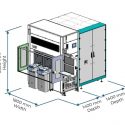
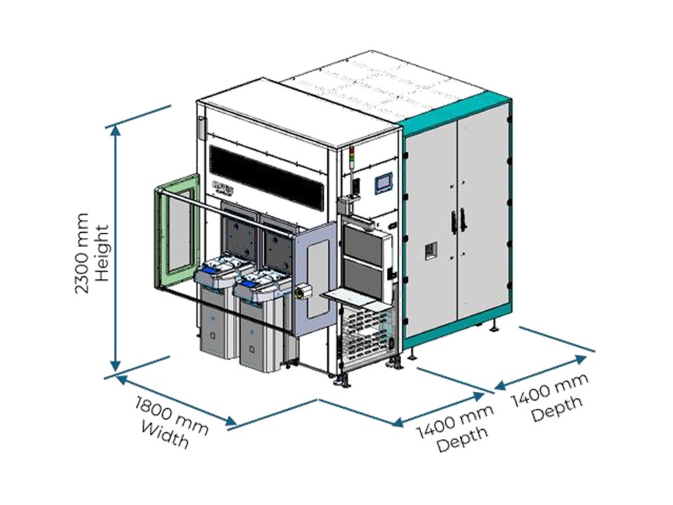
| EFEM-Automatisierungsplattform: | Dual-Load-Port-Modul (N2-Spülung optional) mit Dual-Arm-Roboter. |
There are currently no downloads available.
There are currently no videos available.
- HBM
- TSV
- Gebondeter Wafer
- MEMS (gebondeter Wafer & Kapselversiegelung)
- SSL LED
- Blanker Wafer