


By LUMINA Instruments (DACH, Benelux, North France)
Supplier Info
Product Type:
Metrology & Handling
Application:
Optical Surface Inspection
Product Description:
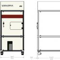
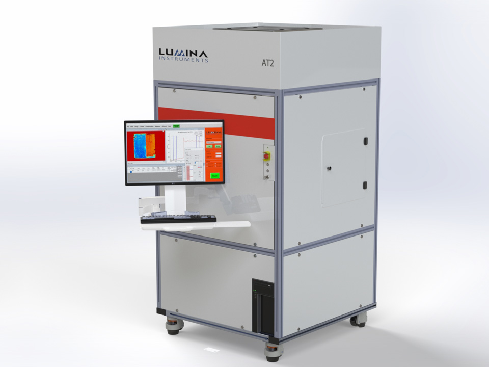
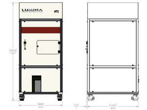
The Lumina AT2 System is capable of scanning any flat shape less than or equal to 450mm x 450mm.
- Resilient: Capable of scanning fragile and thin samples.
- Robust: Dynamic beam tracker enables compensation for substrate bow and warp. Optional bow measurement module is also available.
- Efficient: Full-surface scan of 300mm wafer in 2 minutes.
- Sensitive: 200nm PSL sensitivity on silicon and 300nm PSL sensitivity on glass.
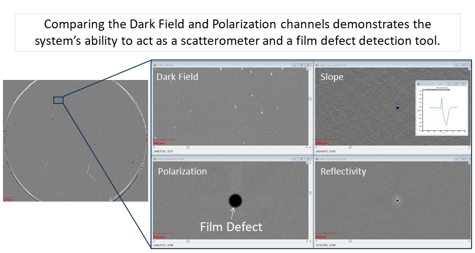
Lumina is working with four detection channels. They operate simultaneously to generate four separate images. Each channel aids in detecting and classifying certain defects:
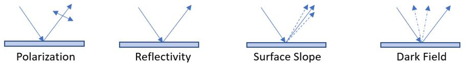
- Polarization: Film Defects, Stains
- Reflectivity: Scratches, Internal Stress*, Striations within Glass*
- Slope: Scratches, Pits, Bumps, Surface Topography
- Dark Field: Nanoparticles, Inclusions
*Reflectivity off of the top and bottom surfaces provides these results.
Related Products:
- The Lumina AT1 System without single arm robot/automated cassette handler for 150 and 200 mm circular wafers.
|
 |
Applications for Glas
Biotechnology, Data Storage, AR/VR, Imprint Lithography, Glass Materials
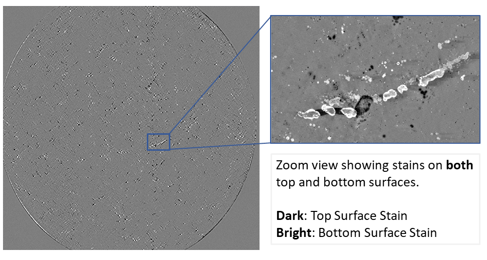
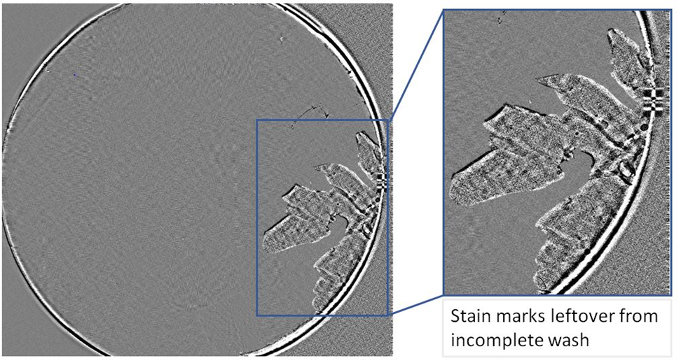
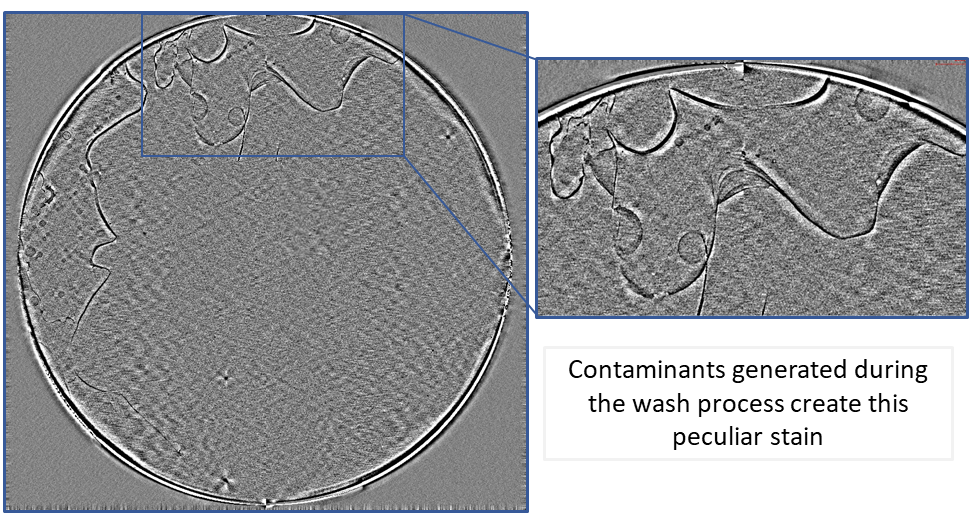
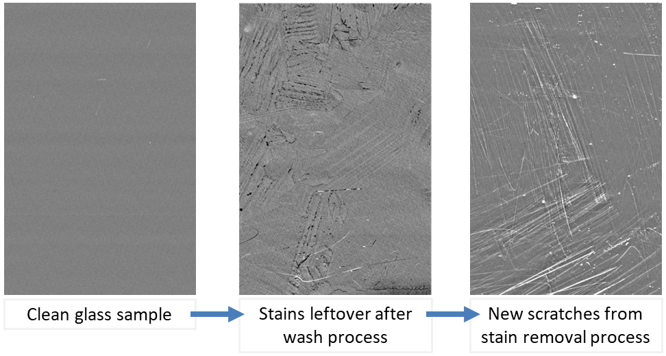
Stains
Stains, or organic residue, are discolorations on the surface due to contamination or residue from the cleaning process. These contaminants not only impact cosmetic appearance, but may also affect the adhesion of coatings onto the substrate.
 |
 |
 |
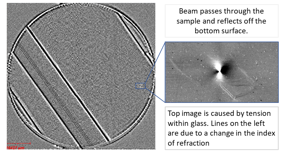
Residual Stress
Residual or internal stress is caused by tension or refractive index variation formed within glass and glass-ceramic materials during production. This can lead to striations, internal defects, and changes in the surface topography. Internal stress is known to impact the mechanical properties of these materials.
 |
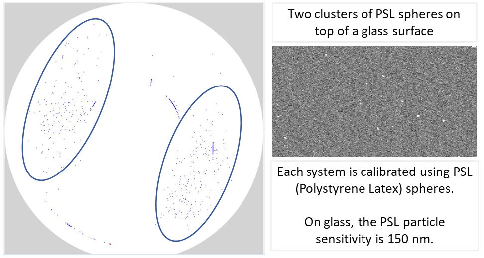
Particles
Particles on the surface of glass can be caused by many factors, usually during the cleaning or packaging phase. Lumina’s systems are able to detect particles down to 150nm on glass surfaces. Controlling particles is critical for achieving high quality and yield. Identifying particles and being able to take action early in the manufacturing process will also help avoid wasting resources on downstream processes.
 |
 |
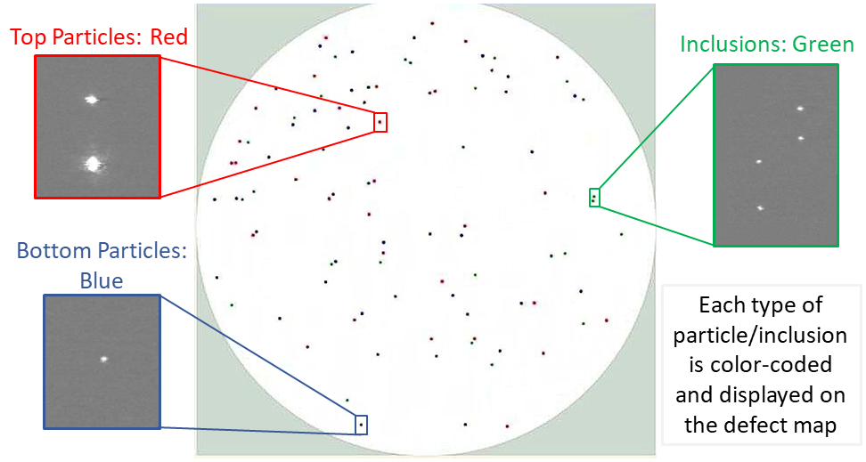
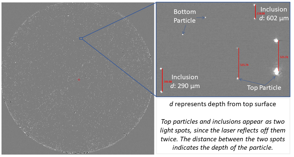
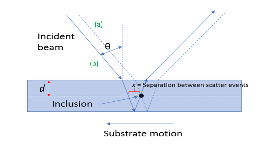
Inclusions and Particles
Inclusions are the result of contaminants incorporated within the glass during the melting phase. These can impact the optical and mechanical properties of the substrate.
There are two methods to detect inclusions:
- Reflectivity: Detecting the residual stress pattern made by the inclusion
- Dark Field: Detecting the double scattering event produced by the direct incident beam (a) and the secondary scattering event (b) due to the beam which reflects from the bottom surface of the glass.
 |
 |
 |
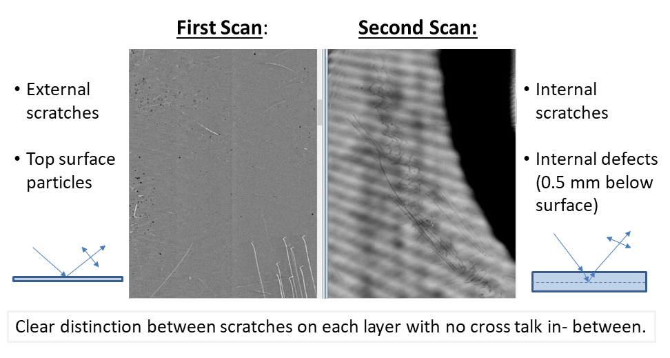
Scratches
These defects can be caused either during the manufacturing phase, cleaning phase, or due to rough handling of the glass. When layers are stacked, internal scratches may occur. Scratches impact the cosmetic and mechanical properties of the glass.
 |
 |
Applications for Semiconductors
Semiconductors, Silicon Wafers, Patterned Wafers
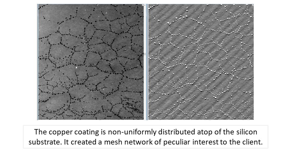
Film Defects
Film defects are typically areas of missing films due to poor coating uniformity due to process conditions or from previous contamination left on the surface before the film was applied. These defects can result in sub-par performance and subsequent yield loss.
 |
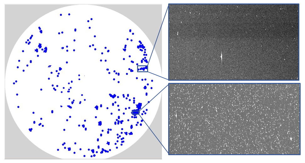
Film Uniformity
Larger areas of film defects can jeopardize the quality of the film layer or coating creating problems with film uniformity. On traditional microscopes, while it may appear that the film is uniform based on a small area of analysis, a full scan on the AT1 system can provide a more comprehensive view.
 |
 |
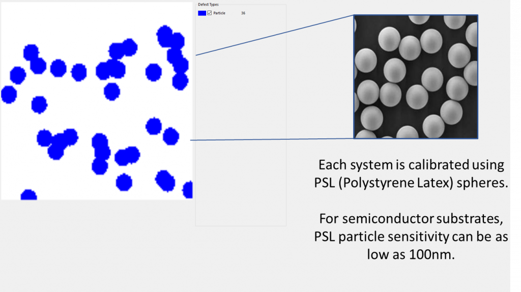
Particles
Particles on the surface of semiconductor substrates can be caused by many factors, usually during the cleaning or packaging phase. Each system is calibrated with PSL spheres on polished silicon. This process demonstrates the instrument’s ability to detect particles down to 100nm.
 |
Applications for Glass Display
Image Sensors, Transparent Conductive Coatings, MicroLEDs
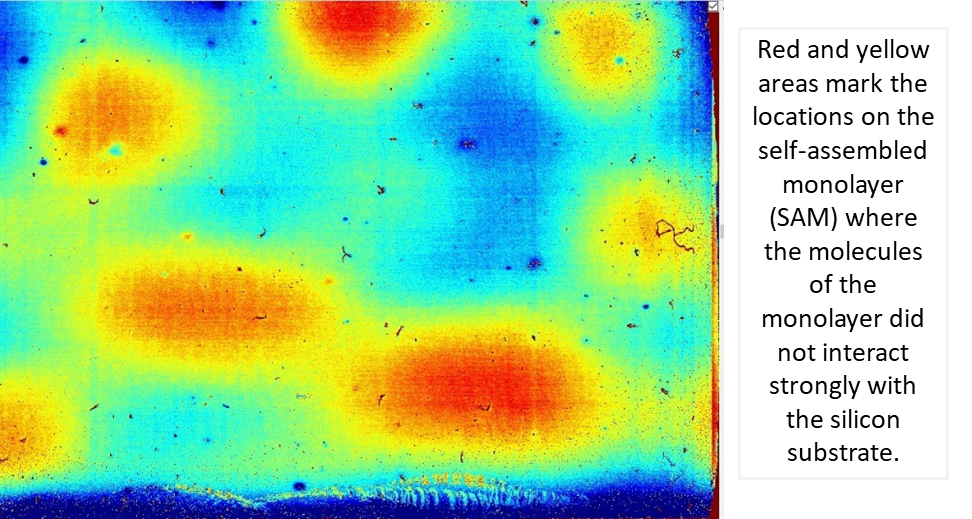
Film on Glass
Lumina Instruments’ tools can be used to analyze local film thickness variation as little as a few angstroms. Detect and analyze films on glass and multiple contaminants that may reside on the surface. Poor film uniformity as well as contaminants can have a detrimental impact on display performance and cosmetic appearance.
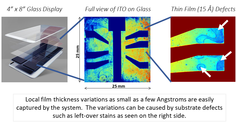 |
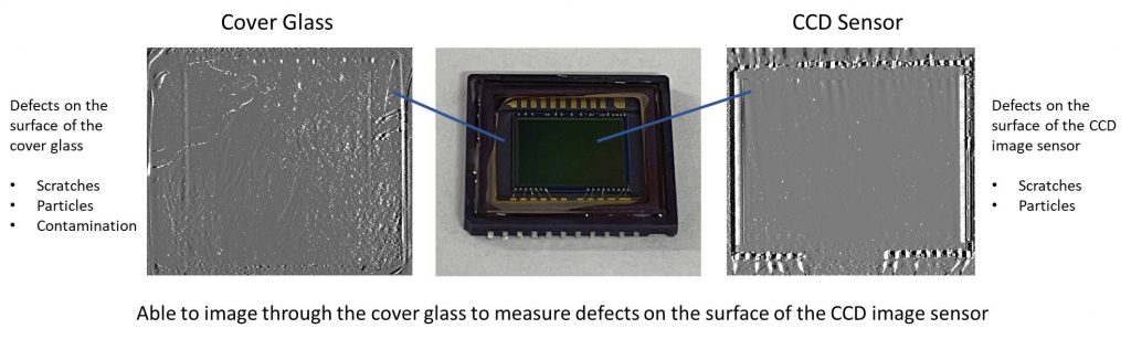
Image Sensors
Detect and classify defects on the surface of both the cover glass and image sensors.
 |