


Product Type:
Metrology & Handling
Application:
H2 Purity Control
Product Description:
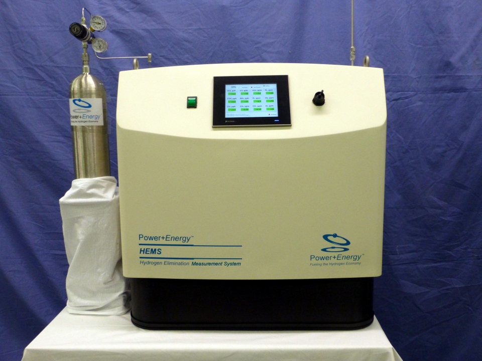
The Power+Energy HEMS™ Hydrogen Purity Analyzer is a full spectrum instrument with limits of detection per impurity of < 1 ppb*. The analyzer is self-calibrating and, with a short analytical cycle time, can be used as an on-line impurity monitor. The compact package and automatic operation make it easy to use for quick sample verification at multiple points.
The HEMS (Hydrogen Elimination Measurement System) analyzer uses P+E’s patented palladium diffusion technology combined with advanced quadrupole mass spectrometry to achieve sub-parts-per-billion resolution.
Compared to other analyzers, HEMS offers detection of the broadest range of impurities in a compact enclosure with automated operation at an affordable cost.
System Specifications
H2 Inlet Purity: ≥ 99.97%
Detection Limit 1 part-per-billion (ppb)
Response Time 5-10 minutes (typical)
Inlet Pressure > 40 psig [2.8 Barg]; 165 psig [11.4 Barg] (typical); Scalable systems upon request
Analysis Flow Rate 2000 sccm (maximum)
Purge (N or Argon) 70 – 90 psig [4.8 – 6.2 Barg]
Connection Types 1/4” mVCR for Vent, Inlet and Purge
Interface 6.5” [16.5 cm] color TFT touchscreen; USB for reporting and maintenance
Environmental 10 – 40°C
Power 100 – 240 VAC, 50/60 Hz
Dimensions 28” x 18.5” x 25” [71.1 x 47 x 63.5 cm] width x depth x height
There are currently no videos available.
Today’s semiconductor manufacturing uses Photolithography in the microfabrication process to pattern parts of a thin film or the bulk of a substrate. It uses extreme ultra violet light to transfer complex geometric patterns from a photomask to a light-sensitive chemical “photoresist” on the substrate. A series of chemical treatments then either engraves the exposure pattern into, or enables deposition of a new material in the desired pattern upon, the material underneath the photo resist.
The complex optical systems used in lithography systems are critical to shrinking the size of microchips. One way to pack more, smaller circuits onto a semiconductor is to use light with a shorter wavelength, such as ultra-violet light. At such narrow wavelengths, regular air would distort the beam path and that is why they are often operated in atmospheres of hydrogen or other gas blends.
When hydrogen atmospheres are used for lithography optics, that hydrogen must be very pure. For monitoring and validating hydrogen quality, engineers can use the parts-per-billion levels of detection found in the HEMS analyzer. The HEMS instrument can continuously sample the hydrogen quality directly from feed lines, eliminating the need for offline measurements performed by scientists in a laboratory.