Category: News

Increase Manufacturing Quality with Reliable Flow Measurement

Implementing Flow Meters Significantly Improves Fab Process Quality

Application image of Semiflow co.65 from Sonotec

Reproducibility and maintaining strict quality control throughout the entire wafer manufacturing process are top priorities in the semiconductor industry. Thus, stable and highly accurate flow measurement is essential for many semiconductor manufacturing steps. Non-contact clamp-on flow meters such as SEMIFLOW CO.65 have proven to fulfill this demanding task reliably.

Semiflow co.65 semiconductor portfolio

The ultrasonic sensors measure through the wall of the tube or pipe and substantially reduce the risk of contamination or leakage of hazardous fluids. With the SEMIFLOW flow meter series, the ultrasound specialist SONOTEC has developed metal-free contactless flow meters particularly designed for the requirements in the semiconductor industry – also for hazardous environments. The compact sensors with integrated electronics board are available in multiple sizes suitable for all common rigid plastic tubes and pipes used in fabs.


Flow Monitoring in CMPSlurry preparationVolume dosing of photoresist


Non-Contact Flow Monitoring in CMP Processes

Reproducibility and maintaining strict quality control throughout the entire wafer manufacturing process are top priorities in the semiconductor industry. Thus, stable and highly accurate flow measurement is essential for many semiconductor manufacturing steps. Non-contact clamp-on flow meters have proven to fulfill this demanding task reliably. The ultrasonic sensors measure through the wall of the tube or pipe and substantially reduce the risk of contamination or leakage of hazardous fluids. With the SEMIFLOW flow meter series, the ultrasound specialist SONOTEC has developed metal-free contactless flow meters particularly designed for the requirements in the semiconductor industry – also for hazardous environments. The compact sensors with integrated electronics board are available in multiple sizes suitable for all common rigid plastic tubes and pipes used in fabs.

In order to guarantee continuous high product quality, a tight liquid flow monitoring is necessary. From liquid storage containers to the application in the process, the liquid flow must be monitored and tracked, e.g., to measure the volume flow in a transfer line or to control the volume output at the points of use. Ultrasonic clamp-on flow meters can be implemented in low- and high-volume manufacturing settings and used reliably regardless of the type or blending of the chemicals in the tube.


Reliable Monitoring of Slurry Consumption in Chemical-Mechanical Planarization
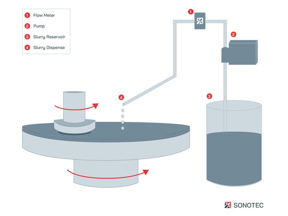
Simplified schematic illustration on a chemical-mechanical planarization (CMP) process with implemented non-contact flow meter from Sonotec

Simplified schematic illustration on a chemical-mechanical planarization (CMP) process with implemented non-contact flow meter


Chemical-mechanical planarization or polishing (CMP) is one of the leading technologies to manufacture state-of-the-art microelectronic components and micro-electro-mechanical systems (MEMS). In order to produce modern integrated circuits with multiple wiring levels and smallest line widths, highly precise flat and smooth surfaces are needed. CMP processes have become also very important in the finishing of wafer-thinning processes and the production of vertical contacts through the silicon wafer.

Since the industry is persistently looking for further ways to reduce the structure width, the requirements in process design are becoming more detailed and stringent. Hence, CMP processes are getting more complex and quality standards grow constantly. As a consequence, process parameters have to be monitored very closely at various steps to avoid deviations in product quality that might lead to costly failures.

In CMP processes, flow meters accurately monitor the dispensing of slurry on the polishing plate. Additionally, they are installed to count the volume flow to calculate the amount of slurry used at this process step. Flow sensors also monitor precisely the consumption of slurry in supply tanks or in the pipe system to determine the transfer volume. Every fab uses its own slurry blending. Non-contact flow meters are well-suited for contamination-free flow or volume measurement of liquids, work independently of the slurry composition and are free of wear and tear.


Fundamentals on Chemical-Mechanical Polishing / Planarization (CMP)

CMP is a key technology in any semiconductor fabrication. It is applied in both, substrate as well as device fabrication. Advanced semiconductor devices easily need more than 30 CMP processes to get to its final stage.

CMP aims on perfect smooth surfaces with almost no remaining topography. To that, the wafer surface is polished using a slurry and a polish pad. Slurry describes a chemical fluid that contains abrasive nanoparticles dispersed in acidic or basic solution. During the CMP process step the wafer is pressed on the rotating polish pad, while slurry is continuously dispensed. Specifically, the slurry chemically modifies the uppermost surface layer, which is then mechanically cracked and removed by slurry abrasives.


Efficient Slurry Blending and Dispensing at Each Point of Use

Large semiconductor manufacturing sites commonly implement slurry mixing and blending systems to ensure optimal slurry concentration for the specific process requirements. For the slurry preparation, the different components are mixed with DI-water. With regard to achieve exactly the predefined slurry concentration at the point of use, highly accurate flow meters monitor the volume flow rate of the components from buffer tanks to the mixing container. This real-time control with contactless flow sensors ensures proper blending of the chemicals at high production rates and specific mixing ratios.

Automatic slurry dispense platforms guarantee an efficient slurry distribution during continuous operations in CMP manufacturing environments. In order to have a redundant system monitoring, non-contact flow meters are installed in addition to each distribution pump to make sure that the defined product quality remains constantly at the same high level. Contactless ultrasound flow measurement guarantees that the slurry or chemical in the pipe or tube is not contaminated or influenced by the measurement device. Additionally, the flow sensor can conveniently be replaced or moved to another position without having to intervene in the closed pipe system.
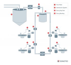
Simplified schematic illustration on slurry management and slurry distribution with implemented non-contact flow meter from Sonotec

Simplified schematic illustration on slurry management and slurry distribution with implemented non-contact flow meter

Slurry Management and Distribution

By monitoring the slurry composition and concentration with automatic dosing and blend correction throughout the entire pipe system, precise metrology options are used. Via additional tank or mixing stations in the fab, blend corrections can be processed. For this step, highly accurate and reliable flow meters control the related pumps. Thus, the exact slurry blending can be ensured and efficiently used. Additionally, flow meters guarantee both system and component redundancy throughout the entire wafer manufacturing process.

In large manufacturing facilities, transfer pumps control the slurry supply via fab-wide loop pipe systems. For redundancy reasons, implemented clamp-on flow sensors monitor the liquid flow or volume in the pipe system.


Precise Distribution of Photoresist in Lithography Applications

In semiconductor manufacturing, the process of photolithography describes the processing of circuit board designs on silicon wafers by means of light. The process starts with coating the wafer with a chemical layer called photoresist. The layer of the photoresist must be extremely precise. For the exact volume dosing of these photoresist layers, highly accurate flow meters are implemented to redundantly monitor the pump behavior. By implementing non-contact ultrasonic SONOCHECK air bubble detectors, even smallest air bubbles can be detected that might occur in the coating process.

In a further step, light passes through a photomask and creates an optical image of the circuit layout on the wafer. The generated light reacts with the photoresist which is washed away in the next process step. Thus, the underlying oxide layer is exposed. By using certain acid baths, further oxide and residues of the underlying silicon layer are removed. As the acid baths have to be kept with an even filling level, non-contact flow meters precisely monitor the filling of the wet benches. Thanks to the non-contact measurement method it is not necessary to replace the sensor after cleaning procedures or servicing. The described process is repeated several times with different combinations of chemicals and masks, building up the layout structure of the later processor.

Finally, the doping process is applied to the exposed silicon, changing its electrical properties. Current photolithography processes often include around 30 or more separate masks to layer circuit patterns on top of each other.


Image © SONOTEC GmbH

Collaboration with Rhosonics

Rhosonics ultrasonic technology for measuring any chemical or solid in production processes.

Collaboration of Rhosonics and S3 Alliance. Handshaking.

We are proud, to announce the news of our collaboration with Rhosonics. A company, based in the Netherlands, in Putten, that has been developing sustainable ultrasonic measuring instruments for process optimization for over 30 years.

Rhosonics design, produce, and supply state-of-the-art ultrasonic sensors and analyzers for various industries, such as the semiconductor industry.

For the semiconductor industry they offer Chemical Concentration Meters. Rhosonics’ ultrasonic technology provides better oversight of the process by simultaneously monitoring multiple chemical concentrations in real-time. The real-time process data allows operators to achieve process optimization in a safe, reliable, sustainable, and cost- effective way. This is a great gain for our customers.

Browse all Rhosonics products

Learn more about Rhosonics

In the picture you see Thomas Riedel (left, S3 Alliance) with Frank Termeulen and Samir Rustamov (Rhosonics).

Heat-Resistant Dicing Tape of NDS

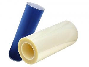
NDS most popular product is the Heat-Resistant Dicing Tape.

Dicing Tape for sale
It is an UV curable type, and even if it is heated up 150 °C in your process for 1 hour, it can easily be peeled from the work after UV irradiation, and there is little generating of an adhesive residue.
The Heat-Resistant Tape “HUV-7000 Series” is available in different types and is suitable for all processes in a clean room.

Check out NDS most popular Heat-Resistand Dicing Tape

Click here for all our NDS products

NDS | S3 Alliance (s3-alliance.com)

Table top SEM CUBE II at the Otto von Guericke University Magdeburg

Otto von Guericke University Magdeburg received a Table top SEM CUBE II from EMCrafts

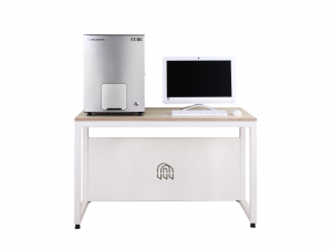
CUBE 2, Tabletop SEM, placed on a table


S3 Alliance has sold and installed an EMCrafts CUBE II scanning electron microscope (SEM) at the Otto-von-Guericke-University  Magdeburg. Weighing only 65 kg, the CUBE II is a very compact tabletop SEM that can be used by the co-workers and students of Prof F. Scheffler’s Industrial Chemistry group, whenever they need a SEM. It is a highly advanced instrument with 5 axes of motion and a resolution of up to 5.0 nm. With optional detectors like EDS (compatible with Oxford, Bruker, EDAX, Thermo), even the chemical composition of various kinds of samples can be explored.
Included are: Auto Rotation, Auto Tilt, Chamber Camera and Navigation. Like this, staff and students can analyze their samples using CUBE II’s simple and intuitive user interface.

The fast imaging capabilities of the Cube II SEM allow for rapid collection of large amounts of data, which is particularly useful for studies requiring large numbers of samples. Dr A. Lieb from the Otto-von-Guericke-University Magdeburg is extraordinarily satisfied with the technical know-how and the commitment of S3 Alliance service technicians on site.

In summary, the Cube II SEM from EMcrafts is a powerful and versatile tool for exploring the micro and nano world. With its high resolution, fast imaging, chemical analysis capabilities, and ease of operation, it is a valuable device for professionals in many fields. It is absolutely forward-looking and exactly the right way for university teaching and research at very affordable costs.


Click for technical details

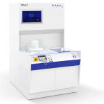
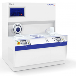
RENA Electroplating Tool EPM 2

Electroplating Tool EPM 2 for Si, GaAs, SiC, Glass and more

Development of new technologies often requires a fast time to market. Therefore process set-up times and flexibility matter as much as perfect quality and meeting customer requirements. With the development of the EPM 2, the RENA manual wet bench for plating applications like UBM, Bumping, Cu pillars, TSVs, RDL, Micro Forming and more we are taking care of your needs.

Features:

  • Outstanding process control and process stability
  • New fountain with multi-zone anodes provides outstanding plating results and a massive uniformity improvement down to 3 %
  • Reduced consumption of additives by up to 20 %
  • Small footprint
  • High process flexibility
  • Easy maintenance
  • SECS/GEM integration

Wafersize: 2“ – 8“
Substrate Materials: Si, SiC, SiGe, Glass, Sapphire, Ceramic, GaN, GaAs etc.
Plating Materials: Cu, Au, Ni, In, SnAg, Sn, Pt, PbSn, FeNi etc.


 See all available Versions:

EPM 2, the RENA manual wet bench for plating applicationsEPM 2, the RENA manual wet bench for plating applicationsEPM 2, the RENA manual wet bench for plating applications

For more information visit our product page
or view all RENA semiconductor MEMS equipment 

Wafer Ashing System from ESI at EPFL, Swiss Federal Institute of Technology

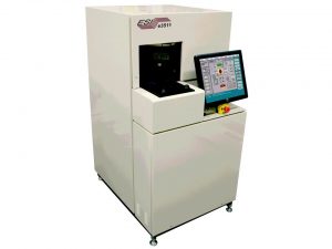
Installation of an e3511 Wafer Ashing System at EPFL, Swiss Federal Institute of Technology

Gasonics e3511 Asher plasma Photoresist stripper. Wafer Ashing System.

Last year, S3 Alliance installed an e3511 Wafer Ashing System from ESI at EPFL, Swiss Federal Institute of Technology. One of Europe’s most vibrant and cosmopolitan science and technology institutions.

The tool was installed inside the Center of MicroNanoTechnology (CMi), a complex of cleanrooms and processing equipment for the training and scientific experimentation devoted to the users of microtechnology.

Mr. Pernollet, process engineer at CMi, stated:
“S3 Alliance installed this tool as complementary to our regular barrel type ashers. Hardware of the e3511 offers us higher rate of resist removal and improved uniformity across wafers which is a real plus for descum processes. The quick and easy handling allows for fast training of our users and the tool proves to be versatile and robust which is a must-have characteristic for our users-based platform!”


See the technical information about e3511

or brows all our products of ESI

ESI, with a focus on serving the semiconductor industry and Gasonic Asher Equipment

Lumina Instruments with Innovative Optical Inspection Systems

Lumina Instruments is a global Supplier of Innovative Optical Inspection Systems

for full-surface defect detection, mapping and classification on transparent, translucent and opaque substrates.

We are proud to introduce our new supplier Lumina Instruments for the area DACH, Benelux and North France. Lumina Instruments is a privately held company with its headquarter in San Jose, California.

With Lumina Instruments, we now offer a new dimension in sustainability, energy savings and best results with innovative Optical Inspection Systems. The system, for full-surface defect detection, mapping and classification on transparent, translucent and opaque substrates.


Experience how the Innovative Optival Inspection System works

Lumina Instruments, Innovative Optical Inspection Systems, Polarization, Reflectivity, Surface Slope, Dark Field


See all LUMINA products

Photography of Lumina AT2-EFEM System

Quantum NXT™ (QNXT) Ultra-Pure Water Heater

    Trebor Quantum NXT (QNXT) save water and energy

Innovation.

Efficiency.

Reliability.

Sustainability.

Based on high end engineering innovation, the Trebor Ultra-Pure Water Heater Quantum NXT (QNXT) provides the required performance with the environment sustainability.


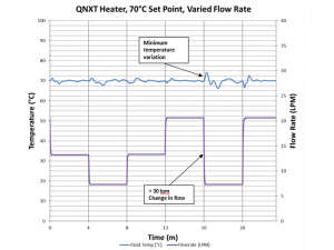
Leading Edge Heating Technology:Trebor Quantum NXT Varied Flow Rate

Patented thin-film on quartz electric resistance heating element provides exceptional temperature response (ultra-efficient heat transfer) and drastically improved reliability, without the necessity of O-ring seals.

Multi-loop PID control with zero crossfire SSRs provide exceptional temperature control.

This proprietary thin-film on quartz has no metal exposure and eliminates contamination risk in the event of element failure. No external air or nitrogen purge is required with the Quantum NXT.


Versatile Control Options:

Multiple communication options are available to meet virtually all unique requirements and protocols. These heaters can be customized to communicate with any wet process tool in the semiconductor industry.


Compact & Convenient:

The modular element allows for very compact system design and can be changed out in less than 15 minutes when required. LCD color touch screen display provides easy user input and diagnostic feedback.


True Eco-Innovation:

The Quantum NXT technology provides both energy and water savings without affecting the demanding requirements of the application.


Ultra Clean Design:

High purity flow path of GE 214 semiconductor grade quartz, PTFE, and PFA with no elastomer O-rings and no NPT threads or dead-legs to create particle traps.


Dual Process Available:

Just one QNXT-D can provide heated DI water for two separate tools, lowering the overall integration cost and saving space, energy and water.


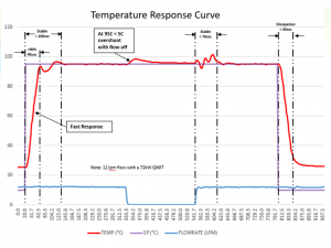
Water Stop Option: Trebor NXT Temperature Response Curve

• Utilizing the Quantum NXT’s Stop-Flow-Technology™, allows near instant heated DI water with next to no waste, allowing to cut off IDLE mode water usage.


Recirculation Option:

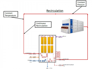
Another unique option offered by the Quantum NXT heater is a recirculation loop for the process water line. This option is the perfect combination of immediate “to-the-point” temperature controlled UPW dispense whenever needed and significant water and energy savings.
Trebor Quantum NXT Recirculation


See all product information about Quantum NXT™


Repair offer of all TREBOR Pumps in Germany

S3 Alliance® Gmbh is a certified Signature Service Provider (SSP) for Trebor Products, which describes the qualification to repair the pumps. We repair all Trebor Diaphragm Pump Models in our workshop in Germany, next to Stuttgart.
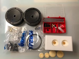
We have not only the facility (wet bench, compressor) and toolsets to pursue this task but also a variety of rebuild kits available for immediate repair out of our stock.

The process steps are as follows:

  • Delivery of a quote for the repair of your Trebor Pump Model (including the rebuild kit that is needed for most repairs)
  • Sending the pump after safe flushing and rinsing together with the Trebor Return Data Sheet
  • Inspection and test run of the pump by S3 to confirm the failure mechanism
  • Disassemble of the pump and evaluation of the defect parts
  • Pre-report sent to the customer to confirm the level of repair chosen
  • Repair after agreement with the customer
  • Test with DI Water and CDA for compliance to the specification
  • Final report and shipping to the customer

TREBOR | Pump repair service

TREBOR | S3 Alliance (s3-alliance.com)


Overhaul of a 300 mm Yaskawa robot by CEK

S3 Alliance® Supplier CEK has recently overhauled a 300 mm Yaskawa robot coming from a semiconductor player in Germany. The equipment engineer stated: “The process went very smoothly and professionally. Compared to the OEM, we were able to save both costs and time without having to accept any loss of quality. Therefore we are planning to use the S3 Alliance® service for our Yaskawa and Kawasaki robots again in the future.”

CEK Technology | S3 Alliance (s3-alliance.com)

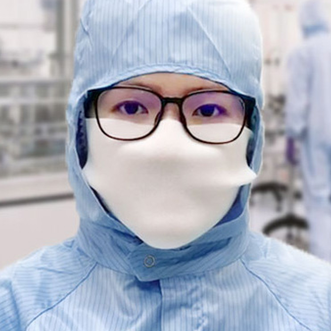
Foamtec Face Masks for Cleanroom

Foamtec’s cleanroom foam face masks are widely employed as under masks in cleanrooms that use headcovers with built-in face masks.

Foamtec’s Foam face masks are not impacted by recently implemented export or import restrictions, so are a more readily obtained mask for semiconductor, pharmaceutical, aerospace and medical device cleanrooms.

Most importantly, the use of Foamtec’s foam face masks does not take supply away from hospitals and medical clinics treating the Corona Virus.

While foam face masks do not have filtration capabilities against viable particulates, the table below demonstrates the low particle counts vs. three-ply non-woven masks. As an added benefit, foam face masks significantly reduce the fogging of safety glasses, primarily when employed as under mask.

LPC

≥ 0.5 um and above

(particles/cm2)

Trial HT4401 3 Ply Mask
1 90 1,567
2 186 1,550
3 168 1,504
Average 148 1,540
Specification < 800 N/A
       

Caption: The table above highlights the particle release characteristics of Foamtec’s foam face masks vs. 3 Ply Non-woven masks.

Browse Foamtec products from our online catalogue

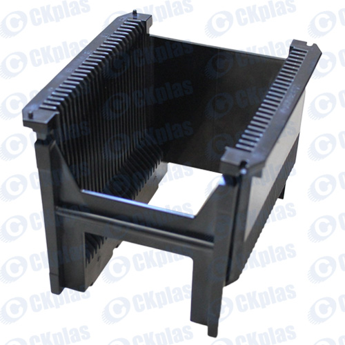
Custom Made 8” PEEK Cassette

At the end of 2nd quarter 2019 S3 Alliance supplied a batch of new custom made 8” PEEK Cassette to one of the biggest IC manufacturers in Russia, Mikron. Cassette was produced under the trade mark CKPlas by our Taiwanese partner – Chung King Enterprise Co. Ltd., located in Taoyuan city. Chung King Enterprise is specialized in wide variety of semiconductor wafer and reticle box from various polymeric materials. Cassette has unique design based on the customer requirements. New, improved raw material (PEEK) has been used for manufacturing of this type of cassette.

Browse all CKPlas products

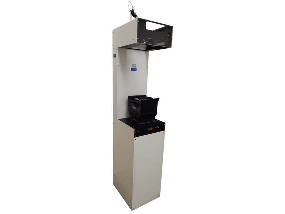
S3 Alliance installed and grounded a Wafer Transfer Unit from Mactronix

Last year S3 Alliance installed and grounded a Wafer Transfer Unit from Mactronix to a Manufacturer of electronic devices in Germany.  The Maintenance Engineer said: 

“Our PVA-TePla Wafer Transfer Units from Mactronix showed increased static load during transfer of ~3KV as measured. The solution offered by Mactronix was to replace the original Ultem combs with new, ESD-compatible PEEK ones. After installing and grounding them (S3-Alliance service available), the measured static load was reduced to <50V!

This solution is simple and very efficient and because the new comb’s pricing is similar to the original combs, also the most price-worthy option to get rid of ESD problems with batch transfer systems in general.”